Equipment for direct writing on wafers 晶元激光直写设备 |
Pattern generators are considered to be complex tools in manufacturing of semiconductor devices. High requirements to such equipment can be met only with the help of high-end technology. KBTEM-OMO has extensive experience in the development of opto-mechanical equipment. The model line of multichannel laser pattern generators for microelectronics built on the raster scan concept is characterized by exceptional functional features: The universality of such high-performance equipment makes it indispensable for scientific institutions and microelectronics manufacturers. EM-5389 Multichannel laser pattern generator |
Equipment for wafer projection imaging 曝光机 |
Equipment for wafer projection imaging is of crucial importance for the mass production in order to decrease cost price of products, therefore the most important parameter of this class of equipment is high efficiency and operational characteristics providing high percent yield. It is completely automated equipment with machine vision systems, high-end software, reprogrammable loading devices. |
Tools for proximity exposure and double-side lithography 双面光刻系统 |
EM-5026xx series and EM-5096 tools are intended for pattern alignment on photomasks and wafers (substrates) and further transfer of this pattern from mask to wafer through contact (proximity) exposure of wafer photoresistive layer.Main features:- wedge compensation and wafer thickness compensation without contact with the photomask;- 3 coordinates (X, Y, Q) high precision wafer manipulator with coarse and fine alignment modes;- ability to handle 0.2 mm to 0.8 mm wafers made of fragile materials (GaAs, LiNbO3) and rectangular substrates;- built-in vibration protection unit;- energy saving mode.
|
Wafer inspection equipment 晶片检测系统 |
The equipment enabling inspection processes is characterized by a large diversity and essentially differs in the degree of complexity: from simple visual inspection tools for mass production to the most complex automatic inspection and measurement systems which are used both in the R& D of new technologies and devices, as well as in the large-scale production. EМ-6419 Wafer flatness inspection system EМ-6429 Automatic patterned wafer micro defect inspection system EМ-6529 Automatic patterned wafer macro defect inspection system EМ-6479 Automatic unpatterned wafer defect inspection system |
Large-area steppers |
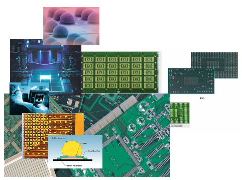
The large-area stepper family is developed by KBTEM-OMO for the flip-chip assembly of high-end chips with numerous output contacts. The flip-chip packaging in many respects determines functional performance of a chip and meets evergrowing demand for higher electrical parameters, further miniaturization, higher reliability, heat and power control at stable cost decrease. EМ-5434 Automatic High Density Integration PCB Stepper EM-5534 Bumping Stepper EM-5634 CCD Stepper |